ABSTRACT
Hybrid two-dimensional photonic crystal structure described by a square lattice of circular air columns with embedded quasi-circular micro-cavities in a square array was fabricated on Si-ZnO substrate using the focused ion beam (FIB) technique. The optical characterization of this photonic device revealed its ability to selectively enhance the reflectance on specific wave lengths in the border of visible-near-infrared range (VIS-NIR). The behavior of the photonic hetero-structure built and studied in this work was attributed to the coupling of the probe light beam with the embedded micro-cavities in the regular square lattice of air columns describing the photonic crystal. The results obtained in this work suggest the presence of a photonic band gap around the border of VIS-NIR range in the studied hybrid photonic structure.
RESUMEN
Se fabricó una estructura fotónica híbrida bi-dimensional mediante el método de haz enfocado de iones (FIB), descrita por una red cuadrada de columnas circulares de aire con un patrón de micro-cavidades cuasi-circulares embebido, describiendo un arreglo cuadrado en un sustrato de Si-ZnO. La caracterización óptica de este dispositivo fotónico reveló su habilidad para mejorar selectivamente la reflectancia en longitudes de onda específicas en el borde de los rangos visible-infrarrojo cercano (VIS-NIR). Este comportamiento de la hetero-estructura fotónica construida y estudiada en este trabajo se atribuyó al acoplamiento del haz de luz de prueba con las micro-cavidades embebidas en la red cuadrada regular de columnas de aire que describen el cristal fotónico. Los resultados encontrados en este trabajo sugieren la presencia de una brecha fotónica prohibida alrededor de la frontera del rango VIS-NIR.
INTRODUCTION
The interest in photonic crystals (PhC) has been growing incredibly in last years since it has been proved that they allow the control the flow of light through materials. Two dimensional (2D) photonic crystals and 2D PhC slabs are of particular interest since several fabrication methods are currently available for this kind of structures. Many applications have been suited to one dimensional (1D) and two dimensional (2D) photonic structures such like antireflective coatings (Domínguez et al., 2012), band pass filters (Robinson & Nakkeeran, 2012), electro-optical sensors (Yang, Tian & Ji, 2011), switches (Rahmati & Granpayeh, 2011), light extraction on LEDs (Zhmakin, 2011) and power splitters (Esmaieli & Ghayour, 2012) just to mention some of them. New applications based on photonic crystals have played a very important role in new advances to develop ultimate technology.
In this work, the fabrication of a two-dimensional hybrid PhC on a silicon (Si) substrate coated with a zinc-oxide (ZnO) thin film of about 240 nm thick is reported. The film of ZnO was deposited onto the silicon substrate in order to control and prevent an excessive damage over the silicon substrate during the irradiation with gallium ions from the focused ion beam (FIB) system. The photonic structure was described by a square lattice of circular air columns with lattice constant a = 1.05 μm and air hole diameter of ~600 nm. The air columns were milled on the Si-ZnO hetero-structure using the FIB technique. This photonic crystal was fabricated with 16 coupled circular micro-cavities embedded in the photonic crystal body with diameter of about 10 μm each. The photonic structure was fabricated with the aim to determine whether the coupling of the micro-cavities embedded within the photonic crystal structure can induce a photonic band gap in the border of the (VIS-NIR) range. The reflectance measurements at normal incidence carried out on this photonic device revealed reflectance selectivity for wavelengths in the border of VIS-NIR ranges. In fact, it was observed a shift of reflectance spectra on our PhC to long VIS wavelengths.
Experimental details
A ZnO thin film ~240 nm thick was deposited on a substrate of silicon wafer by the Assisted Chemical Vapour Deposition (AACVD) method (Amézaga-Madrid et al., 2011). The structure tailored on the Si-ZnO substrate was a square lattice with lattice constant a = 1.05 μm and circular air columns with a diameter of ~600 nm. A pattern of 16 quasi-circular micro-cavities of ~10 μm in diameter and a lattice constant of ~20 μm was embedded in the photonic crystal describing a square lattice. This hybrid structure was fabricated using a Focused Ion Beam JEOL JEM 9320-FIB with Ga+ ion source operated at 26.5 kV. The hybrid photonic crystal was milled on a large area of 84 μm2 × 84 μm2 in order to facilitate its optical characterization. It was necessary to adjust FIB fabrication settings using the spot milling shape to obtain circular patterns since this tool was not enabled with circular geometry for milling. The photonic crystal parameters described above were achieved by setting a dose of 200 nC/μm2 and 1000 pA of irradiating current during 15 s per single hole using the spot milling shape.
Structural characterization was conducted by scanning electron microscopy (SEM) using a JEOL JSM-7401F operated at 2kV. It was observed that during the FIB milling some eroded material was redeposit on the surroundings of holes milled making a rough surface on the photonic crystal area.
Optical characterization of the hybrid photonic crystal was performed by measuring the optical reflectance at normal incidence (Stumpf et al., 2010) using a multichannel fiber couple laser source Thorlabs MCLS1 as a probe light which emits 785 nm, 852 nm and 1550 nm wavelengths. This light source was used to cover discrete broad spectra on VIS and NIR wavelengths with the aim to identify the optical properties of the hybrid photonic hetero-structure. Furthermore, an additional measurement on the hybrid photonic crystal was performed by measuring the reflectance levels across the spatial coordinate x of the PhC by moving the sample mounted in a micrometric linear translation stage. This measurement was carried out in order to identify the contribution of micro-cavities embedded within the regular square lattice on the optical properties of the photonic hetero-structure. The reflectance measurements were taken at normal incidence for all wavelengths using an experimental set up similar to the one described by Stumpf et al., 2010, using a Spectrum analyzer ANRITSU MS9740A. The spot size of the probe light used for this experimentation was measured with a knife-edge laser beam profiler COHERENT BeamMaster Knife, and it was found to be ~15 µm in diameter. Same spot size was used in all experiments reported in this work.
Once reflectance measurements were completed on the hybrid photonic crystal, the ZnO thin film was removed from the substrate surface by means of an acetic acid bath during 30 min. In order to determine the ZnO thin film contribution on the optical properties of the hybrid photonic crystal, the optical characterization of the photonic crystal remaining on silicon substrate was conducted. The optical characterization of this sample was carried out following the same reflectance measurement procedure described above for the photonic hetero-structure in Si-ZnO.
RESULTS
The structural and morphological characteristics of the hybrid photonic crystal fabricated using the FIB milling method developed in this work are shown below in following figures. Figure 1 shows the photonic crystal tailored on a Si-ZnO hetero-structure using the fabrication parameters described above. In addition, it can be observed a section of the photonic device with higher magnification in figure 2 . In order to facilitate the optical characterization, the PhC was milled aligned with the substrate edge. This way, the sample could be properly aligned with the spatial coordinate x when mounted in experimental set up. After ZnO thin film removal it was observed that the topography obtained in the hybrid photonic crystal was transferred to the silicon substrate. In fact, this PhC topography has been predicted in previous theoretical investigations for FIB fabrication method (Han, Lee, Min & Lee, 2010). Figure 3 shows a close view of the photonic structure after ZnO thin film removal.
|
| |
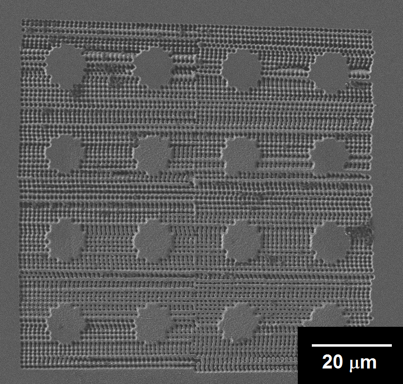 |
Figure 1. Secondary electron SEM micrograph of the hybrid 2D photonic crystal structure milled on Si-ZnO substrate using the FIB fabrication technique.
Source: Authors own elaboration. |
Figure 1. Secondary electron SEM micrograph of the hybrid 2D photonic crystal structure milled on Si-ZnO substrate using the FIB fabrication technique.
Fuente: Source: Authors own elaboration. Close |
|
| |
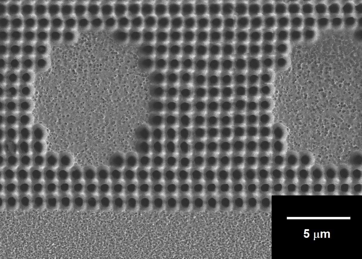 |
Figure 2. Secondary electron SEM micrograph showing a close view of an edge of the photonic device.
Source: Authors own elaboration. |
Figure 2. Secondary electron SEM micrograph showing a close view of an edge of the photonic device.
Fuente: Source: Authors own elaboration. Close |
|
| |
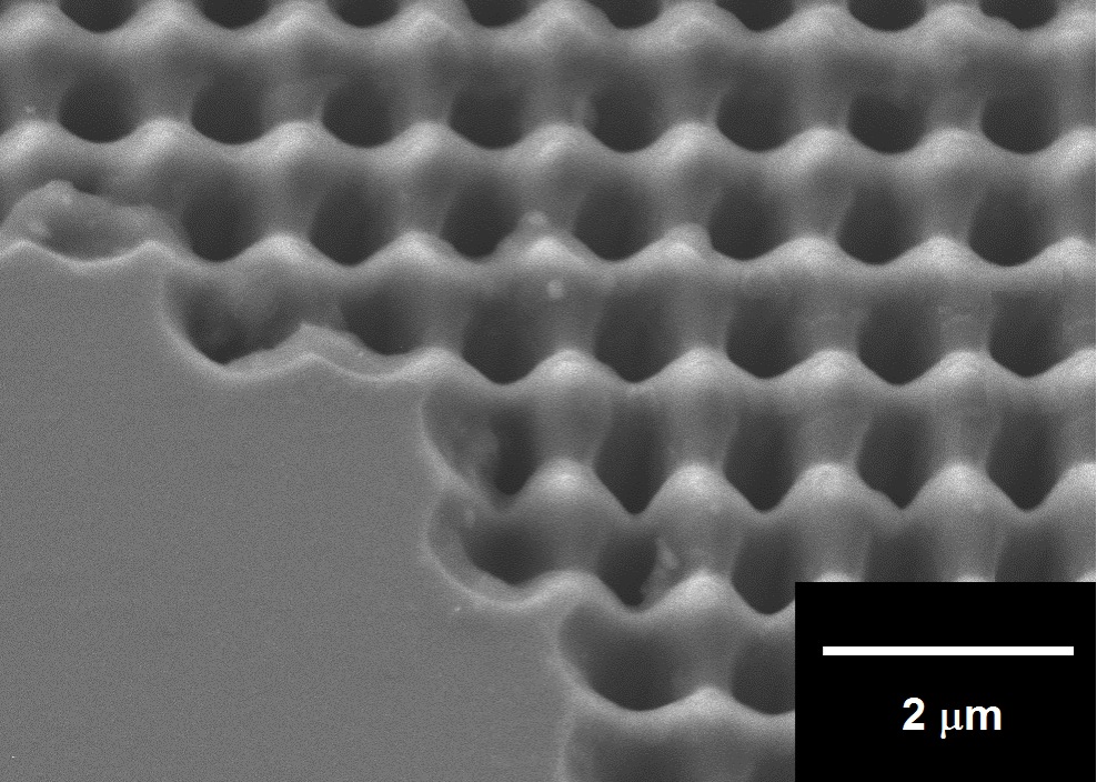 |
Figure 3. Secondary electron SEM micrograph of photonic crystal remaining in bare silicon after ZnO thin film removal.
Source: Authors own elaboration. |
Figure 3. Secondary electron SEM micrograph of photonic crystal remaining in bare silicon after ZnO thin film removal.
Fuente: Source: Authors own elaboration. Close |
The optical characterization of the hetero-structure was completed by measuring reflectance at normal incidence at 785 nm, 852 nm and 1550 nm wavelengths using the experimental set up shown in figure 4. These measurements showed a high reflectance level on the hybrid photonic crystal area at the border of VIS-NIR range wavelengths and a low level for NIR wavelengths. Particularly, reflectance measurement carried out at the beginning of NIR range showed that the level obtained for 852 nm was higher than the level measured at 785 nm on the hybrid photonic crystal as depicted in figure 5. In addition, figure 5 shows the reflectance measurements recorded on the photonic crystal after the ZnO thin film removal. Here, in this case, it was noticeable that the reflectance magnitude was almost constant in the photonic structure on bare silicon for the three probe wavelengths 785 nm, 852 nm and 1550 nm. Also, it was observed that the reflectance level of the photonic crystal on bare silicon only provides a uniform small gain compared to reflectance measured for uniform silicon substrate.
|
| |
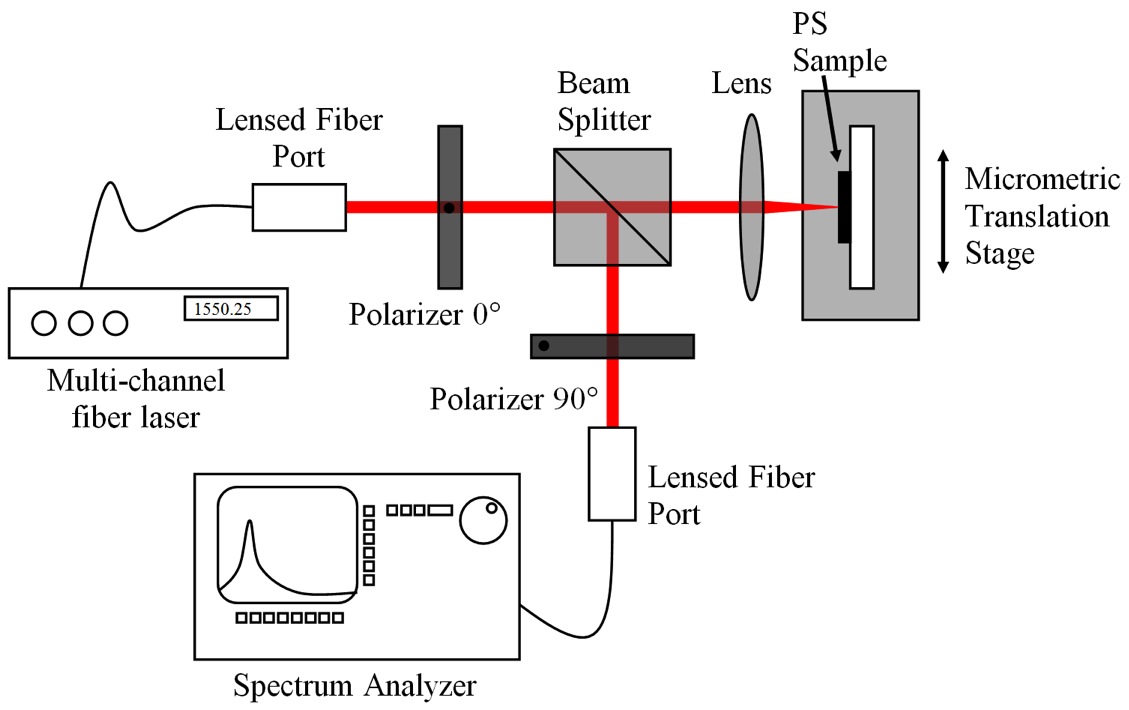 |
Figure 4. Scheme of experimental set up used to measure reflectance at normal incidence.
Source: Authors own elaboration. |
Figure 4.Scheme of experimental set up used to measure reflectance at normal incidence.
Source: Authors own elaboration. Close |
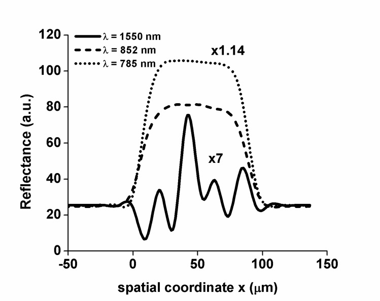
An additional reflectance measurement was taken before removing the ZnO thin film from the silicon substrate to verify if the micro-cavities are coupling to each other with the probe light beam. This measurement was carried out across the spatial coordinate x on the hybrid photonic crystal passing the probe light across the photonic crystal width by means of moving the sample mounted on the micrometric linear translation stage shown in figure 4. Using this method, the probe light is able to pass across and along the cavities and scan all modulations on reflectance level they could produce. Probe light passed from plain Si-ZnO hetero-structure, crossing the photonic crystal to finally reaching the plain Si-ZnO on the other side of the photonic structure. Figure 6 shows the plot of the reflectance levels as a function of the spatial coordinate x. This figure shows a strong modulation on the reflectance level for 1550 nm wavelength which is consistent with the position of the micro-cavities on the photonic crystal lattice. It was observed that the coupling effect of the probe light beam with the micro-cavities in the center of the photonic crystal showed a higher reflectance level than those nearest to the edges. This result was probably due to a partial incidence of the probe light beam on the edges of the PhC and a lesser coupling with the nearest cavities. The described measurement was repeated for 785 nm and 852 nm wavelengths accordingly. Nevertheless, none of these last wavelengths was able to perceive the micro-cavities pattern because they are very small compared to the dimensions of cavities whose magnitude is around 10 microns. Instead of that, the reflectance magnitude for these wavelengths was higher than that obtained for 1550 nm wavelength.
|
| |
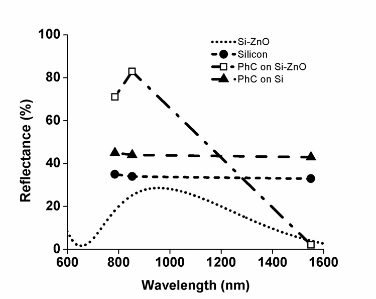 |
Figure 5. Reflectance measurement carried out at 785 nm, 852 nm and 1550 nm wavelengths on photonic structure before and after ZnO thin film removal. Dot line describes the reflectance of Si-ZnO substrate measured by using a spectrophotometer Varian Cary 5000.
Source: Authors own elaboration. |
Figure 5. Reflectance measurement carried out at 785 nm, 852 nm and 1550 nm wavelengths on photonic structure before and after ZnO thin film removal. Dot line describes the reflectance of Si-ZnO substrate measured by using a spectrophotometer Varian Cary 5000.
Source: Authors own elaboration. Close |
|
| |
|
Figure 6. Reflectance profile across spatial coordinate x-axis on photonic Si-ZnO hetero-structure with embedded pattern of 16 micro-cavities using probe light beams of λ=785 nm, 852 nm and 1550 nm wavelengths.
Source: Authors own elaboration. |
Figure 6. Reflectance profile across spatial coordinate x-axis on photonic Si-ZnO hetero-structure with embedded pattern of 16 micro-cavities using probe light beams of λ=785 nm, 852 nm and 1550 nm wavelengths.
Source: Authors own elaboration. Close |
DISCUSSION
In this work it was investigated the feasibility to fabricate a hybrid photonic crystal with an array of embedded micro-cavities in a Si-ZnO hetero-structure containing a regular square lattice of air columns using the FIB fabrication method and its optical properties characterization. The design of this photonic crystal was a square lattice of circular air columns with a lattice constant a = 1 µm and a square lattice of 16 micro cavities of 10 µm in diameter with lattice constant of ~20 µm embedded in the PhC structure. In order to fabricate the photonic crystal using a JEOL JEM-9320FIB it was necessary to use spot milling shape available on the FIB and tune milling parameters to obtain a circular shape.
The structural characterization showed that the photonic structure proposed was successfully fabricated with very good accuracy using the milling parameters as described in previous sections. Also, optical characterization was carried out by measuring reflectance at normal incidence on the photonic crystal. The hybrid photonic structure showed to selectively enhance wavelengths in the border of VIS-NIR ranges rather than NIR wavelengths. In fact, the higher reflectance level at 852 nm probe wavelength was obtained. On the other hand, reflectance measurements on the photonic crystal after remove the ZnO thin film coating showed an almost constant reflectance level. It was found that the photonic hetero-structure slightly increases the reflectance uniformly for all wavelengths probed in the border of VIS-NIR ranges compared to the reflectance measured for silicon substrate.
This indicates that photonic crystal with embedded micro-cavities pattern fabricated on silicon substrate did not contributed in the reflectance modulation as the hybrid Si-ZnO photonic crystal did. Thus, the role of ZnO thin film included in the photonic hetero-structure was relevant for the optical behavior obtained.
Additionally, reflectance measurement was conducted by passing the probe light across the photonic crystal width for all 3 wavelengths used in this work. This measurement showed that the hybrid photonic crystal with embedded micro cavities uniformly enhance reflectance for 785 nm and 852 nm wavelengths. On the other hand, same experimentation showed a spatial reflectance modulation for 1550 nm NIR wavelength.
All these findings clearly indicate that micro cavities were coupled to each other with the probe light beam to provide a reflectance gain at the border of VIS-NIR wavelengths while it spatially modulates the reflectance level for 1550 nm because the latter wavelength is closest to the dimensions of the cavities. Furthermore, it was noticeable that the whole hetero-structure system, i.e. photonic crystal with embedded micro-cavities milled on Si-ZnO, is coupled to selectively enhance the reflectance at 852 nm. This finding suggests the presence of a photonic band gap around this wavelength in the hybrid photonic crystal. This statement has to be confirmed in further experimentation including the measurements of reflectance of our photonic structure sweeping in a continuous way in a region around the border of VIS-NIR wavelengths.
CONCLUSIONS
Two statements could be concluded from this work. First, a hybrid photonic crystal fabricated on a Si-ZnO substrate describing a regular square lattice of circular air columns with embedded quasi-circular micro-cavities in a square array and dimensions as described in this report was able to promote the magnitude of reflectance at the border of VIS-NIR wavelengths range. As it was observed, the photonic structure provides a strong modulation of the reflectance at normal incidence on NIR wavelengths across the photonic crystal width. This modulation of NIR wavelengths found in the hetero-structure fabricated on Si-ZnO substrate could be attributed to the coupling of the probe light beam with the micro-cavities array on the regular PhC described by the square lattice of circular air columns. These findings suggest the presence of a photonic band gap around the border of VIS-NIR wavelength range for the photonic crystal structure reported in this work. On the other hand, last conclusion is on regards ZnO thin film contribution on the reflectance measurements obtained in this study. These measurements also suggest that the coating of ZnO included in the photonic hetero-structure helps to improve the reflection in silicon based photonic crystals.
ACKNOWLEDGEMENTS
The authors want to thank José Ocón Arellanes, and the Thin Film Lab group at Centro de Investigación en Materiales Avanzados (CIMAV) for depositing the ZnO thin film on silicon wafer, and Laboratorio Nacional de Nanotecnología for its participation on PhC fabrication and for help on SEM imaging.
REFERENCES
Amézaga-Madrid, P., Antúnez-Flores, W., Ledezma-Sillas, J. E., Murillo-Ramírez, J. G., Solís-Canto, O., Vega-Becerra, O. E., Martínez-Sánchez, R. & Miki-Yoshida, M. (2011). Synthesis, microstructural characterization and optical properties of undoped, V and Sc doped ZnO thin films. Journal of Alloys and Compounds, 509(1), S490-S495.
Cabrini, S., Carpentiero, A., Kumar, R., Businaro, L., Candeloro, P., Prasciolu, M., Gosparini, A., Andreani, C., De Vittorio, M., Stomeo, T. & Di Fabrizio, E. (2005). Focused ion beam lithography for two dimensional array structures for photonic applications. Microelectronic Engineering, 78, 11-15
Domínguez, S., García, O., Ezquer, M., Rodríguez, M. J., Lagunas, A. R., Pérez-Conde, J. & Bravo, J. (2012). Optimization of 1D photonic crystals to minimize the reflectance of silicon solar cells. Photonics and Nanostructures-Fundamentals and Applications, 10(1), 46-53.
Esmaieli, A. & Ghayour, R. (2012). Magneto-optical photonic crystal 1 x 3 switchable power divider. Photonics and Nanostructures- Fundamentals and Applications, 10(1), 131-139.
Freeman, D., Madden, S. & Luther-Davies, B. (2005). Fabrication of planar photonic crystals in a chalcogenide glass using a focused ion beam. Optics Express, 13(8), 3079-3086.
Han, J., Lee, H., Min, B. K. & Lee, S. J. (2010). Prediction of nanopattern topography using two-dimensional focused ion beam milling with beam irradiation intervals. Microelectronic Engineering, 87(1), 1-9.
Rahmati, A. T. & Granpayeh, N. (2011). Kerr nonlinear switch based on ultracompact photonic crystal directional coupler. Optik-International Journal for Light and Electron Optics, 122(6), 502-505.
Robinson, S. & Nakkeeran, R. (2012). Investigation on two dimensional photonic crystal resonant cavity based bandpass filter. Optik-International Journal for light and electron optics, 123(5), 451-457.
Stumpf, W. C., Asano, T., Kojima, T., Fujita, M., Tanaka, Y. & Noda, S. (2010). Reflectance measurement of two-dimensional photonic crystal nanocavities with embedded quantum dots. Physical Review B, 82(7), 075119.
Yang, D., Tian, H. & Ji, Y. (2011). The properties of lattice-shifted microcavity in photonic crystal slab and its applications for electro-optical sensor. Sensors and Actuators A: Physical, 171(2), 146-151.
Zhmakin, A. I. (2011). Enhancement of light extraction from light emitting diodes. Physics Reports, 498(4), 189-241.